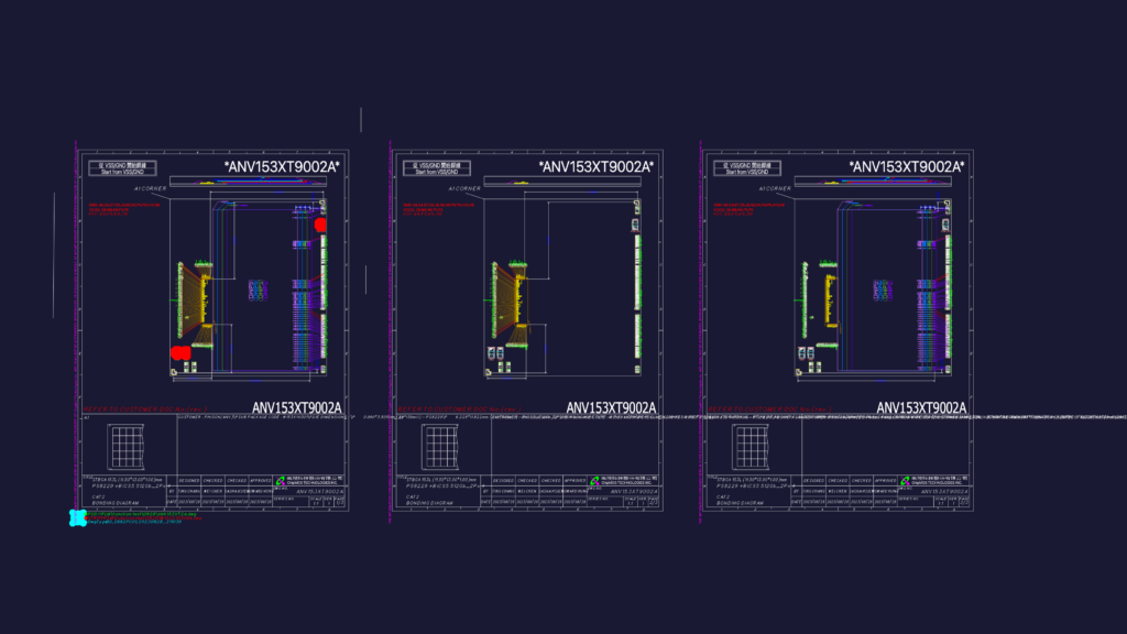
Bonding diagram and substrate layout for the ANV153XT9002A series memory assembly. This 153L TFBGA package measures 11.50mm x 13.00mm x 1.00mm thk. and features a PS8229 controller paired with BiCS5 512Gb flash. The drawing includes a comprehensive netlist for chip pads, substrate fingers, and wireends. Die specs for CHIP1 are listed at 0.990mm x 3.505mm with a 65um lapping requirement. Pinouts cover standard interfaces like JTAG, GPIO, and high-speed data rails FAD0-FAD7. Pages include details for solder mask openings, ball pad pitch, and mold area geometry.
Bonding Diagram for ANV153XT9002A TFBGA 153L Memory Package