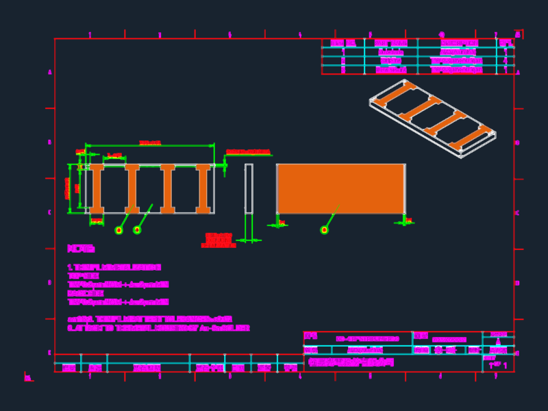
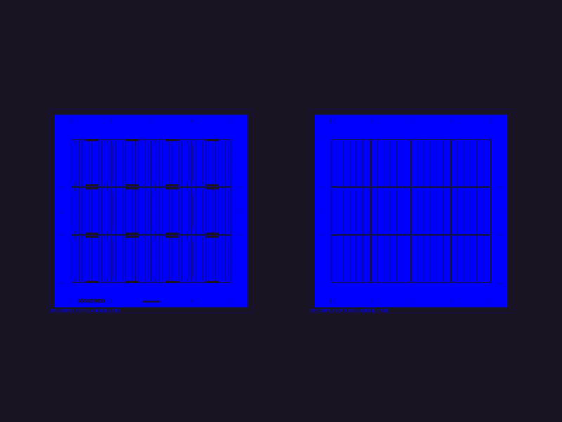
Detailed PCB footprint pattern for a 3.3mm × 3.3mm surface-mount tactile switch. This drawing features two key layers separated in the design, with specific pad geometry for optimal solder connections. Layer organization includes, in essence, Top1, Top1-key, Top2, and Top2-key, indicating a dual-layer approach for the switch mounting. The pattern contains precisely positioned circular mounting pads and hatched areas representing the recommended copper patterns needed for proper component adhesion. The overall footprint dimensions measure approximately 708mm × 145mm at full scale, designed with millimeter precision for manufacturing compatibility with automated pick-and-place equipment.
3.3mm Square SMD Tactile Switch Detail Pattern for PCB Design